
Speed and passion, quality first
To accelerate innovation and safeguard qualityOur end-to-end service is a highly collaborative and seamless' highway '
Date:2026-11-19
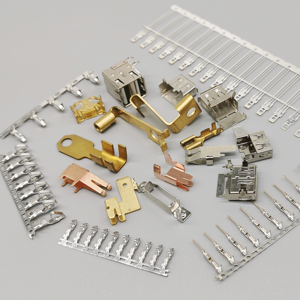
Short answer: hold the process, not the measurement. A terminal that measures 6 mΩ on the bench and 14 mΩ after 500 mating cycles was never actually at 6 mΩ — the test did not reproduce the service condition. Four process variables decide whether the number holds: burr at the contact zone, plating thickness uniformity, spring temper consistency, and contamination.
Most contact resistance disputes come from measurement, not from the part.
| Requirement | Why it matters |
|---|---|
| Four-wire (Kelvin) measurement | A two-wire multimeter includes lead and probe resistance, which can exceed the value you are trying to measure |
| Dry circuit condition | Test voltage must be low enough that it does not break down the surface film. A high test voltage "measures through" the oxide and reports a resistance the application will never see |
| Specified test current | Different currents give different results on the same part |
| Clean, unmated surfaces | Finger oils and handling contamination add film resistance |
| Defined mating position | Measuring at partial insertion gives a meaningless number |
If a supplier reports contact resistance without stating the method, the number is not comparable to anyone else's.
A burr on the contact surface concentrates current into a smaller real contact area and can also prevent full seating. Burr height is a direct function of die condition and punch/die clearance — it drifts as the tool wears. This is the most common cause of a part that passes first article and fails three months later.
Control: specify burr height and direction on the drawing; monitor burr at fixed intervals, not only at tool launch.
Plating resistance is in series with contact resistance. Thin spots — at edges, inside bends, in high-current-density areas of the plating bath — raise resistance locally and become the first point of wear-through.
Control: specify plating thickness as a range with a minimum, measure at defined locations including bend radii and edges, and require the certificate to trace to the production lot.
Contact resistance is a function of normal force, and normal force is a function of the material's temper and the formed geometry. Incoming strip with temper variation outside the specification produces terminals that look identical and measure differently.
Control: specify temper by hardness range, verify incoming material certificates, and include a spring-force check in the control plan — not just a dimensional check.
Micro-motion at the contact interface repeatedly breaks and reforms the oxide layer. The debris is insulating, so resistance climbs while the part shows no visible wear. Fretting is driven by vibration amplitude and thermal cycling, not by mating cycles.
Control: contact geometry that maintains force under thermal expansion; plating systems resistant to fretting (gold over nickel, or tin with sufficient force and wipe); vibration testing as part of validation.
Cutting oil, plating bath residue, and handling contamination all add film resistance. A part that measures well immediately after assembly can fail after storage.
Control: specify cleanliness, control storage and packaging, and test after any cleaning or storage step — not only on freshly made parts.
| Symptom | Likely cause | Process control |
|---|---|---|
| Resistance high at first article | Burr, contamination, insufficient normal force | Burr spec + cleanliness + spring-force check |
| Resistance fine at first article, drifts over months | Tool wear increasing burr; plating wear-through | Interval burr monitoring; plating thickness minimum |
| Resistance rises after thermal cycling | Stress relaxation reducing force; fretting | Material temper selection; vibration/thermal validation |
| Resistance varies between lots | Incoming strip temper variation; plating bath drift | Incoming inspection; plating certificate traceability |
| Resistance varies within a lot | Plating thickness distribution; handling damage | Plating location sampling; packaging review |
Contact resistance should be treated as a process characteristic with a control chart, not as a final inspection gate. Practical setup:
A single pass/fail gate at the end of the line tells you that a problem exists. A control chart tells you when it started.
BOSI stamps precision terminal connectors with:
For fine-pitch terminals, the constraint is usually not the press but the interaction between burr, plating and measurement. Those three are reviewed together at the DFM stage.
Have a terminal that must hold a resistance limit over life, not just at first article? We will review geometry, plating and the measurement method before tooling.


 Language
 Your location:

.jpg?x-oss-process=image/resize,m_pad,h_176,w_262)


 Official account
 0769-82928019
 E-mail
